How are the varieties of NAND flash memory categorized? What type is best for your embedded design? We help you answer these questions, and we examine how software can improve the longevity of your chosen NAND type.
In earlier materials, we compared NAND and NOR flash directly. Data size and usage, performance strengths, and the storage management software were all factors in choosing the media. While NOR continues to be a stable platform for booting and storing certain data, the storage size continues to grow slowly. Storage improvements, primarily in NAND based media, have outperformed Moore’s law by a factor of 800%. This makes it a great choice when you need to store large quantities of data on your design.
In this article, we will discuss some of the NAND improvements and what they mean for firmware and flash translation software. We’ll take a look at how the different types of NAND flash memory compare, and which to consider depending on your embedded use case.
Bits per cell – a key factor
A major aspect differentiating types of NAND flash memory is “bits per cell.” As data is stored on NAND flash memory in the form of “bits,” this refers to the number of “bits” of data held on each cell of a NAND types.
Bits per cell is an important characteristic because it’s critical in balancing performance, robustness, and cost in your NAND-based design. And as NAND flash memory has evolved over the years, the bits per cell count has been a key factor that has changed.
A quick history of NAND types
We’ve just taken a look at how some of the main NAND types differ in bits per cell, but how did this happen?
When first invented, NAND and NOR cells stored a single bit each, based on the amount of charge in the cell.
NAND designers soon realized that instead of measuring against just one threshold, they could measure against three – storing two bits in a given cell. With a thought towards the future, this was referred to as a Multi Level Cell (MLC). The single bit solution was called Single Level Cell (SLC).
Later designs stored three bits per cell, and still later four bits per cell. These were technically still MLC, but not quite as exciting on a marketing data sheet. Thus, TLC and QLC were born, without the acronym translating to anything specific.
These clever design solutions were not without a cost, however. Higher bits per cell can result in a greater bit error rate – and a reduced maximum Program and Erase (P/E) count. Storing more bits also results in less silicon overall, reducing the raw costs.
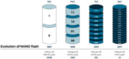
Take a look at the image above for a quick breakdown of how bits per cell has evolved.
Again, as a general rule of thumb, the more bits per cell the lower the cost of the flash, but you need to buy more of it in one go while compromising on some speed and durability.
You will notice that the image uses a lot of 1’s and 0’s in its notation. How does a flash memory controller determine whether a cell has a 1 or a 0 anyway? This is done by measuring the amount of electrical charge in a given cell. A freshly erased cell has a 1 – when programmed beyond a certain threshold, it is now considered a 0.
Now let’s look at the different types of NAND flash in more detail, and things to consider when evaluating which flash to use in your design.
Single bit per cell (SLC)
The most basic type of NAND flash memory is single-level cell (SLC) NAND. Storing 1 bit per cell, it has the fastest read and write speeds of any NAND type, while also having the longest lifespan.
SLC is commonly used in industrial applications where high performance and reliability are critical. It is however the most costly form of NAND memory because of its low bit per cell count.
Harsh environmental designs are among the places that SLC NAND flash thrives. Additional bit errors due to temperature conditions are easily handled, and the extra cost in P/E cycles is not enough to affect the overall lifetime. At this time, all SPI NAND flash is of the SLC type.
Whitepaper: Data reliability in space
Space is one of the harshest environments for NAND flash. Read about some of the ways that flash can be made to last longer in our whitepaper, “Data reliability in space.”
Multiple bits per cell (MLC)
In terms of data bit count, MLC NAND is a step up from SLC, featuring two bits per memory cell instead of just one. Due to this increased bit density, MLC has more bit error potential over SLC, higher error correction requirements, and reduced endurance.
MLC NAND can deal with a moderate amount of program and erase (P/E) cycles. In general, this type of NAND provides a good balance between performance, lifetime, and cost. It can be a suitable choice if your design would benefit from that balance. That could mean anything from a programmable logic controller (PLC) to a telematics control unit in the vehicle, or a robotic control unit.
One thing to note about MLC is that its performance and lifetime can vary depending on the actual temperature of its operational environment. This can be an important consideration if you are developing a device that may be required to operate in extreme temperatures.
Power interruption while writing to an SLC write page will corrupt the page being written. On all MLC NAND flash, it also has the potential to corrupt data on a second ”paired” page. In this situation, a power interruption can undetectably corrupt a file that is not being operated on.
Flash media vendors strongly recommend a capacitor or other means to maintain power during a page program operation. This and other programming requirements are the primary reason why Linux flash file system developers have given up on supporting MLC NAND flash.
TLC and QLC flash
We’re covering TLC and QLC flash together, as they serve largely the same market, and there are a lot of similarities in their attributes.
TLC NAND stores three bits of data per memory cell, while QLC stores four. As a result of this increased bit count, they are both more cost-effective than MLC, but they do sacrifice some endurance to get there. This endurance shortage is due to a couple of things, such as:
-
- Having so many bits stored on a memory cell. As each bit of data contains an electrical charge, the combined voltage of all those bits can ultimately increase the likelihood of bit errors on the memory cell. The endurance drop in QLC is more severe than in TLC NAND due to the bits being packed even tighter on the QLC memory cell.
- Increased wear during P/E cycles, as a result of having the bits of data packed so closely together on the cell.
- Lower total P/E cycles overall, compared to other varieties of NAND flash. This is a consideration if you foresee that your embedded design will need to face high numbers of writes.
Knowledge of use case is among the most important design considerations for TLC and QLC flash media. File systems with large write amplification can result in heavier flash usage – directly counter to the low total of P/E cycles.
In designs where flash writes are strictly controlled, TLC or QLC flash can be an excellent choice. They also receive heavy use in consumer designs that have a short expected lifetime – thumb drives for example.
Related content:
Curious to learn more about how write/erase cycles affect the lifetime of NAND flash memory, and what to do about it? Read our article, “Automotive flash – what’s the real lifetime?”
Getting the most out of your flash memory with a flash memory manager
Whichever type of NAND flash you decide to use in your embedded design, it is important to ensure that you are getting the most performance, reliability, and lifetime out of your chosen memory. A key way to do this is to implement a flash memory manager. In short, this is a piece of software or firmware that helps to organize the data in your flash memory storage device.
An excellent choice for your flash memory management is Tuxera FlashFX Tera. We have engineered it to help you achieve the fullest lifetime and reliability in your flash-based design, regardless of the specific type of NAND that you may be using.
The wear-leveling algorithms used by FlashFX Tera make a huge difference in preventing uneven cell usage on the flash, which goes a long way to extending the lifetime of the memory. In addition, error correction codes and patented bad block technology ensure that your flash-based data stays uncorrupted. This is a huge boon for any kind of flash-base design – especially if you decide to go with a bit-heavy memory type (like QLC) for your design. Remember, FlashFX Tera is the only Linux solution that supports MLC NAND flash.
Final thoughts
NAND flash is the most likely design choice for very large data storage needs – and there is a lot to consider when selecting the right NAND for your design.
The key differences between many NAND flash memory types are in their cost, performance, endurance, and use cases. SLC offers the best performance and longevity but is the most expensive. As you move to MLC, TLC, and QLC, the cost decreases, but endurance and performance become progressively lower.
When evaluating which type of NAND flash is most suitable for your embedded design, think carefully about the requirements your use case. Everything from the size of the device to the temperature of the environment that it will operate in can have significant effects on the lifetime of the flash memory being used.
You will likely want to implement a flash memory manager that is built to ensure that your chosen NAND option remains robust and long-lasting. Proper design in both hardware and software are needed to get the most performance and lifetime from all NAND, especially MLC.
Whitepaper: Avoid end of life from NAND correctable errors:
Learn more about extending the lifetime of NAND flash memory in our whitepaper, “How to avoid end of life from NAND correctable errors.”